wut??
On this page a translation of the italian documents will be produced. As there are several people working on this, a wiki seems to be the right place to do it. After finishing a translation, we will produce a PDF of the results and publish it on the web using a Attribution-Share Alike licence as the information herein is of crucial inportance in fixing these early personal computers.
The original pdf is from museotecnologiamente.it
Introduction to the Logic Schematics
Olivetti Programma 101 Legenda fogli logici famiglia P101
Ivrea 6 Marzo 2010 Gaiti Giuliano
Introduction
Due to the fact that the Logic Papers on the Olivetti Programma 101 were made in 1965 using a now complete obsolete schematic representation, an introduction to the schematic symbols used is necessary. The original seven logic sheets are redrawn on a computer to improve readability and differ only marginally from the originals.
The main component on the Printed Circuit Boards (PCBs) and in the schematic is the micromodule. It consists of a small PCB on which the components (resistors, capacitors and diodes) are arranged vertically in two rows, with one end soldered to the small PCB of the micromodule, and the other end soldered on the main board when the micromodule is installed on it. If there is a transistor used in the module, it is soldered entirely on the micromodule PCB.
NOR
The logic function represented in the figure is a 5-input logical NOR, its inverse function creates an AND between the signals LA * TA * SH * KB * PO \. The generated signal is VO1. The name of the signal is typically limited to two letters of the alphabet, followed by a number:
- TRUE, straight, signal generator.Odd number starting from 1 as first generator, followed eventually by 3, 5..
- FALSE, negated, signal generator.Even number starting from 2 as first generator, followed eventually by 4, 6..
On the schematics it doesn't appear the number of the legs on which signals are applied due to the fact that it is being used the convention of counting the signals from the top down and attribute them to the respective pins of the "micro-module P101" of reference, mounted straight.
The NOR micromodules can have 3 or 4 rows; the transistor is always mounted in the top 2 rows, and with the reduction to 3 rows the number of inputs diminishes.
The location of the micro-modules on the PCB, is indicated with 5 characters, for example 01F30, that mean:
- 01 > printed circuit board
- F > column
- 20 > row
Since every column on the PCB has 2 rows of holes, the reference is always the top left pin on the components side. (PCB seen from the component side, and edge connectors down). regardless of the mounting position of the Micromodule, being upright or upside down.
In case the micromodule has brougth out the base of the transistor directly, an input is sacrificed that will always be the last among those available.
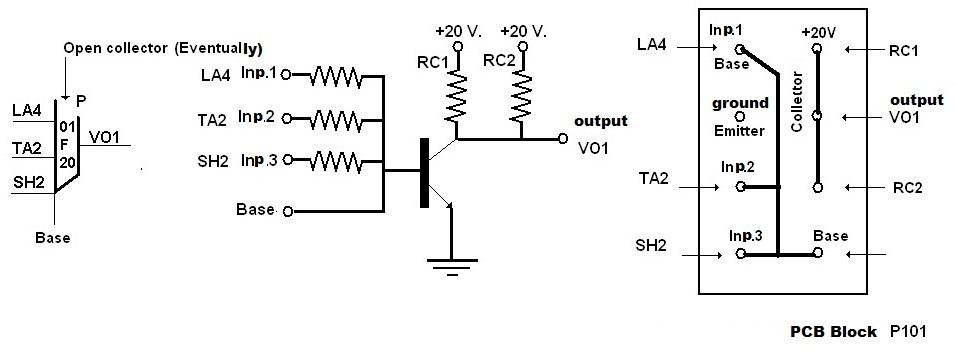
In the case of NOR, open collector, the collector resistance is not connected to the power supply. On the schematic the open collector is indicated by the lack of a diagonal line on the top of the trapezoid representing the NOR.
In case of fan-out, requirement for driving a high number of inputs, due to the power dissipation the number and value of the resistor to power (+20 volt) is varied. On the schematic the highest power is indicated by a letter P.
The example shows three versions of the same module. Left the schematic representation, middle the electronic equivalent and right the PCB layout of the micromodule.
The need to have controlled and quick switching is handled by selection of different transistors. Micro-modules with a fast transistor are identified by the letter V.
A 3-input NOR is used for the logic function of the inverter. The two superfluous inputs may have been left unconnected or more likely connected to Ground.
In the original schematics the unconnected inputs are not drawn in. On the new fabricated schematics the unconnected inputs are indicated by the letter Z.
Flip Flop
There is only one type of flip flop, achieved by connecting two NOR (2 micro-modules) to intersection.
The NOR used can be of different types, both for the number of inputs, outside availability of the base and fan out (normal, power or speed). The flip flop can switch either via signals applied to the inputs (resistors), or from circuits shunts connected to the base of the transistor, in slang called masks.
The figure represents a flip flop driven by both inputs and masks.
The symbol of the Flip Flop is a rectangle, divided into three sections, of which:
• Left NOR whose output is the side True = 1 of the Flip Flop (Straight). Bears the mounting indication of the correspondent micromodule. • Central Eventual ndication of type of circuit (V, P, 2P). • Right NOR whose output is the side True = 0 of the Flip Flop (Denied). Bears the mounting indication of the correspondent micromodule.
At the base of the rectangle, in bold, the name of the flip flop is shown.
The extensions at the corners of the rectangle representing the Flip Flop indicate: • Left Side 1. High (If any). Connects the base of the transistor on the side Set - Straight of the Flip Flop to additional circuits, typically masks or additional resistive inputs. Set the Flip Flop. 2. Low Indicates the signals applied to the resistances of the same NOR. Reset the Flip Flop. • Right Side 1. High (If any). Connects the base of the transistor on the side Reset - Denied of the Flip Flop to additional circuits, typically masks or additional resistive inputs. Reset the Flip Flop. 2. Low Indicates the signals applied to the resistances of the NOR on the Negated side of the Flip Flop . Reset the Flip Flop.
It is noted that the signals applied to the resistors saturate the transistor, while the signals applied to the derivative masks act only on the falling edge, elapsing it. The resulting effect is that the signal applied to the resistance on the left side resets the flip-flop, while the signal applied to the capacitor of the mask, on the same side, sets it. Conversely, the signals applied to the resistors on the right side set the Flip Flop, while the signal applied to the capacitor of the mask resets it. The application of commands contemporaries and opposite, makes indeterminate the operation of the Flip Flop.
Masks
The mask circuit is represented by a circle having, eventually, inside a letter that specifies the type (see different types of Flip Flop). On the diameter of the circle (horizontal), are drawn two segments indicating the the first the signal which controls the switching of the flip flop on the capacitor and the second, the connection of the diode output to the base of the transistor. The condition signal, enable = 0, it is typically placed at the base of the circle or with a vertical segment, if the condition signal is missing, the resistance is connected to ground so that the mask is always enabled. Each micro-module contains two masks of the same type, identified by the letters A and B.
Each of the two masks has the components aligned vertically. Mounted upright, the micromodule presents from the top diode, resistance to power, resistance with a condition and capacitor of Mask A, on the left side. On the right side are the components of Mask B. The position 02G28 indicates that the micro-module, when mounted upright, will have the diode pf Mask A (XV1) in column G line 28 of the circuit board 02.
Buffer circuits or filter
The buffer circuit (resistances) and filter (RC groups) are presented as rectangles having as base the shorter side, divided in two parts. The left side, with the micromodule installed upright, indicates the type of circuit by a code, ZB15 for example. The right side denotates the mounting position of the micro-module on the PCB.
(: pcb 06, column C, row 20) not existing
Oscillators, Monostable Circuits and Amplifiers
Typically, these circuits are made of multiple micromodules. In the example, a monostable circuit, the number of micro-modules is 3. The first rectangle contains only the name of the circuit, in our case OP. The three micro-modules are represented by the next three rectangles underneath each containing the installation position on the PCB. Eventual input and output signals are shown on the relative micromodule and with their pin number.


